课程大纲
- 涵盖微纳制造技术的核心工艺,包括:
x 外延(Epitaxy)
x 氧化(Oxidation)- 扩散(Diffusion)
- 离子注入(Implantation)
x 化学气相沉积(CVD)
x 物理气相沉积(PVD)
x 光刻(Lithography)
x 刻蚀(Etching) - 化学机械抛光(CMP)
- 集成(Integration)
- 封装与测试(Packaging and Testing)
- 微电子技术的核心是硅基集成电路制造。
- 集成电路与分立器件的区别:
- 集成电路需要隔离工艺和金属互连工艺。
- 集成电路工艺更复杂,对单工艺要求更高。
Lecture 2: Epitaxy
外延工艺,指在晶体上用化学或物理方法规则地再排列所需晶 体材料。外延层与衬底晶向相同,但掺杂类型、电阻率、材料可以不同。外延生长的层是有序的,而PVD的层是随机长多晶/非晶,CVD则可以生成多晶/非晶与单晶(外延CVD)
1. 外延可以做什么?
- 外延双极型晶体管:高集电结击穿电压,低集电极串联电阻
- 双极型电路的pn结隔离
- 衬底上先外延,再在上面做CMOS电路,可以避免闩锁效应,避免硅层中SiOx的沉积,使得硅表面损伤小
2. 外延可以分为?
- 按材料分
- 同质(均匀)外延
- 异质(非均匀)外延:异质外延外延层与衬底的相容性要求在外延温度不发生化学反应、不互溶,热力学匹配,晶格匹配
- 失配率计算
- 按工艺方法分
- 气相外延 (Vapour Phase Epitaxy):以气相形式把材料输运至衬底,高温下分解或发生化学反应,在单晶衬底上生长出与衬底取向一致的单晶外延层
- 硅的外延: \(\begin{matrix} \left. \begin{array}{r} \mathrm{SiCl}_4\\ \mathrm{SiHCl}_3\left( \mathrm{TCS} \right)\\ \mathrm{SiH}_2\mathrm{Cl}_2\left( \mathrm{DCS} \right)\\ \end{array} \right\} +\mathrm{H}_2& \rightarrow \mathrm{Si}+\mathrm{HCl}\\ \left. \begin{array}{r} \mathrm{SiH}_4\\ \mathrm{Si}_2\mathrm{H}_6\\ \end{array} \right\}& \rightarrow \mathrm{Si}+\mathrm{H}_2\\ \end{matrix}\)
影响外延生长速度的因素
- 外延温度:低温时,外延速率主要受表面外延过程控制;高温时,外延速率主要受质量传递过程控制。其实低温也可以实现气相扩散,高温下化学反应快,将温度控制在高温区,目的是降低温度波动对生长速率的影响
- 硅源种类:有Cl的更慢
- 外延剂浓度:硅源浓度超出临界范围生成多晶硅,甚至硅衬底被腐蚀
- 衬底晶相:(111)共价键密度低,成键能力差,外延层生长慢,而(110)较快
- 反应器形状尺寸,外延气体流速流量
- 外延掺杂: \(2\mathrm{PH}_3\left( \mathrm{H}_2 \right) \rightarrow 2\mathrm{P}+5\mathrm{H}_2\uparrow\) 还有$\mathrm{B}_2\mathrm{H}_6,\mathrm{As}\mathrm{H}_3$
掺杂剂需要用氢稀释十~五十倍,以减小掺杂气体的流量误差 原位气相掺杂:将掺杂剂以气态形式与主材料前驱体 同步引入反应室,实现原子级别的均匀掺杂 杂质掺入外延层浓度依赖于:外延气流中掺杂剂分压,外延温度、速率,反应器几何形状,掺杂剂自身特性
掺杂浓度分布:8-30,8-32 自掺杂效应(self-doping effect):掺杂衬底中的杂质反扩散进入气相边界层,又从边界层扩散掺入外延层的现象,是气相外延的本征效应,不可能完全避免 内扩散效应(inter-diffusion effect):衬底与外延层中的杂质,在外延过程中相互扩散,引起外延界面附近杂质浓度缓慢变化。在高温外延时,会引起外延界面附近杂质浓度的再分布 改进的办法:
- 降低工艺温度,用低温硅源
- N衬底外延前埋层掺杂,使用蒸汽压、扩散系数都低的杂质,如锑
- 重掺杂衬底,先用轻掺杂硅薄层密封其底面和侧面,减少杂质外逸
- 低压外延,可以抑制自掺杂效应


- Low Voltage Epitaxy (8-35)
- Selective Epitaxy (SEG) (8-36)
- Silicon On Insulator (8-37)
- 液相外延 (8-44)
- 固相外延 (8-46)
- 分子束外延 (Molecular Beam Epitaxy): 物理气相外延,低温超高真空度下,热分子束由喷射炉喷出,射到洁净的单晶衬底表面,用于外延层薄、杂质分布复杂的多层外延
- 气相外延 (Vapour Phase Epitaxy):以气相形式把材料输运至衬底,高温下分解或发生化学反应,在单晶衬底上生长出与衬底取向一致的单晶外延层
- 还有一堆
- 按温度分:高温(1000以上),低温(1000以下),变温(先低温下 成核,再高温下生长外延层)
- 按电阻率分:正外延,低阻衬底上外延高阻层;反外延,高阻衬底上外延低阻层
- 按外延层分:普通外延,选择外延,多层外延
- 还有:按结构划分;按外延层厚度划分
3. 外延层缺陷与如何检测
位错,层错 硅衬底的各向异性与低温、快速生长、高压导致漂移与畸变
Lecture 3: lithography
先讲光刻的指标要求,再讲工艺是怎么满足要求的
1. 光刻的要求
- High resolution
- High sensitivity of photoresist
- Low defect
- High multi of mask alignment
- Own the ability to process large size wafer for lithography
2. 光刻系统的主要指标
- 分辨率(Resolution):
- the ability of an optical system to accurately distinguish between targets
- Rayleigh’s Law:$R = k_1\frac{\lambda}{NA}$,$k_1$ 为Resolution factor (phase shift), $\lambda$ (DUV 193nm - EUV 13.5nm), $NA$ 为Numerical Aperture (Immersion lithography)
- Minimum line width $L=\frac{1}{2R}$ limited by diffraction $L\ge\lambda/2, R_\text{max}\le 1/\lambda$
- 焦深(Depth of Focus, DOF):
- the optical difference between the light rays on the axis to the limiting focus position 光刻胶表面能够清晰成像的垂直范围。
- Rayleigh criterion: $DOF=\delta=\pm k_2\frac{\lambda}{(NA)^2}$
- 对比度(Contrast):
- 定义:光刻胶上光强分布的陡峭程度。
- 高对比度有助于形成清晰的图形。
- 线宽控制(Linewidth Control):
- 定义:光刻胶上线宽的均匀性和一致性。
- 影响因素:曝光剂量、显影条件、光刻胶特性。
- 对准精度(Alignment Accuracy):
- 定义:多层光刻中不同层图形的对准精度。
- 重要性:影响器件的性能和良率。
- yield, and price.
3. 光刻三要素 Three elements of Photolithography
- 光刻胶(Photoresist):
- 正胶(Positive Photoresist):曝光区域溶解,适合高分辨率图形。
- 负胶(Negative Photoresist):曝光区域不溶解,适合大线宽图形。
- 特性:Resolution, Sensitivity, Adhesion and viscosity, Stability
- 掩模版(Mask Plate):
在透明基底上蒸镀Cr图形, 在Cr图形上覆盖anti-reflection coating- 1 Selection of glass substrates: small expansion coefficient, high transmittance in the range of wavelengths and high stability against dissolvents to withstand the multiple exposure cycles without degradation or deterioration. glossy surface, no protruding points, depressions, scratches and bubbles, flat layout, moderate and uniform thickness.
- 2 Prepare glass substrate: cut and mill plate glass
- 3 Evaporation of chromium film: proper film thickness, high uniformity, minimal defects such as pinholes or contaminations, and high firmness
- 光刻机(Photolithography Machine):
- 组成:光源、光学系统、对准系统、工作台。
- 光源
graph LR; A[Hg -220nm contact/proximity] B[DUV 250-110nm scanning projection] C[VUV 65nm step projection] D[DUV 45-14nm immersion step scanning projection] E[EUV 14nm-] A-->B; B-->C; C-->D; D-->E;- 光学系统
- 接触式光刻 contact: 分辨率高但掩模版与光刻胶膜易损
- 渐进式光刻 proximity: 掩模版与晶圆保持一定距离, 分辨率下降 (edge diffraction and surface reflection)
- 投影式光刻 projection: 用光学系统投射形状, 最常用的 (scanning, step-and-repeat)
- 多重曝光技术:通过多次光刻和刻蚀实现更小的特征尺寸 (double pattern density)
- Lithography-Etching-Lithography-Etching: 双倍分辨率,两次曝光各自独立会产生套刻误差,且第二次曝光-刻蚀的基底是不平整的
- Lithography-Freeze-Lithography-Etching: 双倍分辨率,两次曝光一次刻蚀,套刻误差,第一次显影碱性影响第二次光刻胶
- Self-Aligned-Quadruple-Patterning: 双倍分辨率, 一次曝光,复杂,不适应任意图形
mask->die->feature的图形变换
- 分辨 PR positive/negative
- 分辨 mask clear field/dark field
4. 光刻工艺流程
在黄光超净间中,
- substrate preparation wash -> bake -> tackify (HMDS increases the adhesion of PR to wafer)
- 涂胶(PR Coating):
- 将光刻胶均匀涂覆在硅片表面。
- 方法: manual, auto spin, auto spray
- 控制参数:转速、胶液粘度、环境温度。
- 软烘(Soft Bake / pre bake):
- 去除光刻胶中的溶剂,提高粘附性。
- 方法: hot plate conduction, infrared radiation, drying circulating hot air
- 对准曝光(Alignment and Exposure):
- PR undergoes photochemical changes and form latent image
- The exposure time is determined by the intensity of the light source and the type and thickness of the photoresist
-
后烘 (bake after exposure)
- 显影(Development):
- spray or immersed in the developer -> part of PR dissolve -> development inspection under a microscope
- 显影液 developer:碱性溶液(如 TMAH)
- factors: ① exposure time, ② pre-baking temperature and time, ③ photoresist film thickness, ④ developer concentration, temperature, ⑤ developer stirring and so on.
- 硬烘(Hard Bake):
- 提高光刻胶的机械强度和抗刻蚀性。
- 烘烤温度比之前更高
- development checking:
- check PR drilling/etching
- check graphic size changes, registration alignment, flush/steep lines
- check defects (pinholes, island)
- PR removal:
\(\begin{cases} wet\begin{cases} negative\,\,PR:98\%H_2SO_4+H_2O_2+PR\rightarrow CO+CO_2+H_2O\\ positive\,\,PR:acetone\\ \end{cases}\\ dry\begin{cases} O_2+PR\xrightarrow{heat}CO+CO_2+H_2O\\ plasma\left( O^++O^- \right) +PR\rightarrow CO+CO_2+H_2O\\ \end{cases}\\ \end{cases}\) - final checking:
- first, surface visual inspection for smudges and large contamination
- then, microscopic inspection / automated inspection for defects and deformations
5. 光刻技术的前沿发展
- 采用不同的光源:
- E-beam: 用低能密度电子束, high resolution, easy creation and modification of graphics, short production cycle, 会出现散射效应和临近效应
- X-ray: 用高能电子束轰击靶材产生X-ray, mask很薄
- Ion beam: 分离选择10keV以下的离子束用于刻蚀与外延, 10-70keV用于曝光
- 浸没式光刻(Immersion Lithography):
- 在光刻胶与镜头之间加入液体(如水和PFPE),提高 NA 和分辨率
- Nano Imprint Lithography
- 微接触印刷, 热压印, 紫外压印
- 无掩膜光刻(Maskless Lithography)
- 电子束/激光聚光, 可编程扫描
Lecture 4: Oxidation and doping
1. 二氧化硅薄膜
- property: crystal structure, density, …
- 二氧化硅(SiO₂)是集成电路中的关键材料,用于掩模、钝化保护、电隔离等。
- 考虑掩膜:impurity diffusion coefficient $D_{SiO_2}=D_0e^{-\Delta/kT}$。对掩膜的厚度和扩散系数要求$x_{min}=4.6\sqrt{D_{SiO_2}t},D_{Si}\gg D_{SiO_2}$
2. 热氧化 Thermal oxidation
- 氧化工艺类型:
- 干氧氧化(Dry Oxidation):$Si+O_2\rightarrow SiO_2$致密、生长慢。
- 水汽氧化(Water Vapor Oxidation):$Si+\left( H_2+O_2 \right) \rightarrow SiO_2+H_2$疏松、生长快。
- 湿氧氧化(Wet Oxidation):$Si+H_2O\left( O_2 \right) \rightarrow SiO_2+H_2O$介于两者之间。
- 因此对于mask oxidation (thick), dry-wet-dry; 对于MOS gate oxidation (thin film), dry / chlorine-doped oxidation, 流程是wafer cleaning -> increase temperature -> growth -> wafer pick up % 对厚氧化层分多次生长,避免通孔
- 氧化层厚度计算:
- 产物SiO2和原料Si的厚度比:$d_{Si}=\frac{n_{SiO_2}}{n_{Si}}d_{SiO_2}=\frac{2.2\times 10^{22}}{5\times 10^{22}}d_{SiO_2}=0.44d_{SiO_2}$
- 干氧和湿氧的厚度比。
- Deal-Grove模型:描述氧化层厚度与时间的关系。
| quasi-equilibrium steady-state growth | $x^2 + Ax = B(t+\tau)\rightarrow x_{_{SiO_2}}=\begin{cases} \frac{B}{A}(t+\tau ), t\rightarrow 0\ \sqrt{B(t+\tau )}, t\rightarrow \infty\ \end{cases}$ |
|---|---|
| Oxidant transport | $F_1=h_g(C_g-C_s)$ |
| solid-phase diffusion | $F_2=\frac{-D_{SiO_2}}{x_0}\frac{\partial C}{\partial x_0}=D_{SiO_2}\frac{C_0-C_i}{x_0}$ |
| chemical reaction | $F_3=j_sC_i$ |
| Reaction by-products leave the interface |
| factor | effect |
|---|---|
| temperature | $k_s, D_{SiO_2}, h, \dots \sim T$ |
| oxidant partial pressure | $B\propto P$ |
| crystal orientation | $A\sim$, (111)is the fastest and (100) is the slowest; |
| impurity | $Na, Cl, H_2O,$ III, IV, trace impurities $\uparrow$ |
3. 实际的氧化
D-G模型不能精确描述 thin oxidation, 真实的氧化也不是连续的, 存在initial oxidation(快速初始氧化)等多个阶段. 以MOS gate为例讲thin oxide的流程:
- requirement: low defect density, good barrier resistance to impurity diffusion, low interfacial state density and fixed charge, high quality SiO2/Si interface, good stability under hot carrier stress and radiation.
- Process method: dry oxygen oxidation, or chlorine doped oxidation; vacuum oxidation; Low temperature and high pressure oxidation
- Process conditions: slow enough; thorough Cleaning; ultra-high purity materials.
氧化过程中杂质的重分布: Impurities/Dopants separate and redistribute during oxidation, with separation rate of $K=\frac{n_{Si}}{n_{SiO_2}} \sim T, \text{crystal orientation}$
氧化层质检
- oxide thickness measurement: Colorimetric method ($d=\frac{\lambda}{2n}x$), interference fringe method, Ellipsometry, step meter
- Film forming quality inspection: Surface defects, structural defects, charge in the oxide layer, thermal stress.
4. 掺杂工艺
- 扩散(Diffusion):高温下杂质原子在硅片中的扩散。
- 离子注入(Implantation):通过高能离子束将杂质注入硅片。
Lecture 5: 刻蚀技术
1. 刻蚀参数 (思考:如果不满足会怎么样?)
- 刻蚀速率(Etching Rate):单位时间内去除的薄膜厚度。 $ER = \Delta h/t$
- 刻蚀因子(Etching Factor):刻蚀深度与横向扩展的比值。 $F = V/\Delta X$
- 选择性(Selectivity):刻蚀目标材料与掩模或衬底的刻蚀速率比。 $S_R = \frac{E_f}{E_r}$
- uniformity: Intra-chipuniformity, intra-lot uniformity and inter-lot uniformity.
- etching cleanliness: residues, polymers, particle contamination
刻蚀要求怎么样
因此有Good uniformity of etching,Good fidelity of graphics, High etching selectivity ratio, High cleanliness of etching, Processing large batches
2. 刻蚀工艺有哪些
- 湿法刻蚀(Wet Etching):各向同性,适合大线宽。
- 步骤:reactants diffusion -> reactants react -> reaction produce diffuse
Advantages High selectivity ratio ($S_R$) No substrate damage Simple Good uniformity large batch Disadvantages Poor cleanliness Low resolution and fidelity (isotropic) Defects (exotherm -> temperature rise, gas bubbles generated -> reactance stoppage) 影响因素 photoresist adhesion, SiO2 property and impurity, etching temperature, time, 溶液浓度和搅动 - 例子: \(\begin{matrix} SiO_2:& \begin{array}{c} 6HF+SiO_2\xrightarrow{NH_4F}H_2\left[ SiF_6 \right] +2H_2O\left( iso \right)\\ Si+2KOH+H_2O\rightarrow K_2SiO_3+H_2O\left( aniso \right)\\ \end{array}\\ Al:& 2Al+6H_3PO_4\rightarrow 2Al\left( H_2PO_4 \right) _3+3H_2\\ \end{matrix}\) 注意:各向异性刻蚀对单晶硅的 (111) 速率远大于 (100),溶剂有各种碱和有机EPW、TMAH、EDP 刻完记得水洗干燥
-
干法刻蚀(Dry Etching):各向异性,适合高精度(sub-micro)。
| Category | description |
|—————-|—————————————————-| | sputter | accelerated ions physically knock out material ($F$) | | plasma | plasma chemically react with film ($S_r$) | | reactive ion etch |sputter + plasma | | high-density plasma etch | …还有Magnetic Field Enhanced Reactive Ion Etching (MERIE), Inductively Coupled Plasma Etching (ICP), Electron cyclotron resonance plasma etching (ECR)|- 刻蚀剖面是各向异性,具有较好的侧壁控制;最小的光刻胶脱落或粘附问题;好的片内、片间、批次间的刻蚀均匀性;较低的化学品使用和处理费用
- 例子:
\(\begin{matrix}
SiO_2:& CF_4\xrightarrow{plasma}C + F^*, SiO_2+F^*\rightarrow SiF_4\uparrow + O_2\\
Al:& BCl_3 \xrightarrow{plasma} B+ Cl^*, Al + Cl^* \rightarrow AlCl_3\\
W: & CF_4 \xrightarrow{plasma} C + F^*, W + F^* \rightarrow WF_6\uparrow
\end{matrix}\)
- 刻蚀Si/SiO2:
plasma 里面掺点杂质有什么用? 比如用CF4刻蚀,掺O2提升刻蚀Si和SiO2的速率(ER),但降低SR;掺H2会显著降低刻蚀Si的速率,略降SiO2,SR会改善 目前 SiO2 用 CHF3 刻蚀,掺一点O2, SF6 and NF3 are used to increase the fluorine content
- 刻蚀多晶硅:chloride and bromide (aniso), fluoride (iso)
为什么多晶硅刻蚀分两步? 1 Siliconize the metal with CF4, SF6, Cl2 or HCl -> 2 engrave polycrystalline Si with Cl2 +Ar . the rate of etching polysilicon is much faster than that of siliconized metal; the etching of polysilicon sidewalls should be avoided.
- 刻蚀氮化硅:LPCVD Si3N4 is as a selective oxidizing mask,CF4,or CF4(+O2 、SF6、NF3) is as the etching gas; PECVD Si3N4 is as device protection film, etching of pressure-soldered joint windows with CF4+O2 as etching gas.
- 刻蚀Si/SiO2:
3. 最新发展
- 高深宽比刻蚀(High Aspect Ratio Etching)
- 等离子体刻蚀(Plasma Etching)
- 硬掩膜版 hard mask process:先用很薄的光刻胶 干法刻蚀中间层(硬掩膜版),再以中间层为模板 干法刻蚀底层薄膜材料(刻蚀对象),最后湿法清除中间层。解决光刻胶选择性差和倾斜倒塌的问题 移除光刻胶 PR removing:Solvent PR removing (金属),Oxidizer PR removing (没金属),Plasma PR removing
Lecture 6: 化学气相沉积(CVD)
- CVD是通过气相化学反应在衬底表面沉积薄膜的工艺。
- 应用:只要衬底足够平整且能承受高温,制备amorphous/polycrystalline的dielectric film(SiO₂、Si₃N₄)、多晶硅薄膜, 还有tungsten and metal silicides。
- 特点: good adhesion, high comformal coverage
1. 原理
- CVD的过程:
- Gas-phase Mass Transport: The gas mixture enters and forms a “boundary layer” on the wafer surface; Silane diffuses to the substrate surface
- Surface Chemical Reaction Process: decomposed gaseous atom groups become adsorbed molecules on the surface; Surface reaction occurs, the generated silicon atoms in the aggregation-nucleation connect to form a film, H2 is desorbed and expelled from the reactor.
- Grove模型推算反应剂流量低时薄膜淀积速率: \(G\begin{cases} =\frac{k_sh_g}{\left( k_s+h_g \right)}\frac{C_T}{N}Y\\ \approx \frac{C_T}{N}k_sY, \text{表面反应控制过程},\text{对温度敏感(低温)}\\ \approx \frac{C_T}{N}h_gY, \text{气体质量输递控制},\text{温度不敏感(高温)}\\ \end{cases}\) 其中, 反应系数$k_s=k_0e^{-E_A/kT}$, 输递系数$h_g=D_g/\delta$.
- 结论:
- 质量输运控制(反应剂浓度因素): 需要确保气流速率及分布应均匀;对温度控制要求不高
- 化学反应控制(温度因素): 需要温度波动小且分布应均匀;对气流控制要求不高
- 为什么反应物浓度较高Grove模型算的不对:忽略了气态副产物从衬底解吸、扩散出边界层的影响;忽略了反应器室内温度梯度对气相物质输运的影响
compared with epitaxy:
- lower temperature, faster rate
- substrate surface can not be a single crystal
- no epitaxial regular arrangement process or incomplete arrangement, so the precipitated film is amorphous or polycrystalline.
2. CVD薄膜质量控制
- 保形覆盖(Step Coverage):薄膜在复杂结构上的均匀性, 由于到达每一点的反应剂数量不同会有遮蔽效应 (shadowing)
- 应力控制(Stress Control):通过降低薄膜淀积工艺温度等降低薄膜内应力 (internal stress), 区分内拉应力 (tensile) 和压应力 (compressive)
- 薄膜的致密性: 温度越高薄膜越致密
- 厚度均匀性: 衬底温度、气流成分与分布均匀,气体流动状态稳定
- 附着性: 温度越高,附着性越好, 化学吸附/化学键都很牢固
3. CVD工艺类型
为了进一步降低反应温度, 将其他类型能量转为化学能, 就有了那一堆复杂工艺
- 常压CVD(APCVD):设备简单, 快, 适合厚膜, 有微粒污染,台阶覆盖性和均匀性差; 温度控制在气相质量输运限制区
- 低压CVD(LPCVD):可竖立密集摆放衬底, 生产效率高, 有颗粒污染; 但是工艺温度较高,表面反应控制; 有气缺现象, 要沿气流方向逐步提高加热器温度来抵消浓度差
- 等离子增强CVD(PECVD):质量好, 除了薄膜较疏松,密度较低, 氢多点; 适合做SiO2 Si3N4钝化膜和保护膜; 低温, 表面反应控制; 影响淀积速率与质量的因素还有反应器结构,射频功率的强度和频率,反应剂与稀释剂气体剂量,抽气速率
- 高密度PECVD (HPECVD), 金属有机物CVD (MOCVD), 激光诱导CVD (LCVD), 微波等离子体CVD (MWCVD)
- 原子层淀积 (ALD): 用于 高k介质 金属薄膜
Si3N4薄膜与SiO2薄膜比较:
- 抗钠能力强,硬度大,针孔少,更致密,化学稳定性好,作为钝化膜、保护膜有优势;
- 掩蔽能力强,SiO2对B、P、As、Sb有掩蔽作用,Si3N4还可以掩蔽Ga、In、ZnO。能作为多种杂质的掩蔽膜。
- 介电常数ε大、导热性好,作为电容的介质层;
- 与硅失配率大,与Si3N4接触的Si界面缺陷大,成为载流子陷阱,或者复合中心,影响硅的载流子迁移率。
4. 各种材料的沉积
\(poly-Si\begin{cases} SiH_4\left( silane \right) \rightarrow poly-Si+2H_2\\ SiCl_4+2H_2\rightarrow poly-Si+4HCl\\ \end{cases}\) \(SiO_2\,\,\begin{cases} AP\begin{cases} SiH_4+2O_2\rightarrow SiO_2\left( \text{绝缘层} \right) +2H_2O\\ SiH_4+O_2\rightarrow SiO_2\left( \text{绝缘层} \right) +2H_2\\ Si\left( C_2H_5O \right) _4+8O_3\rightarrow SiO_2\left( \text{绝缘层} \right) +10H_2O+8CO_2\\ \end{cases}\\ LP\,\,\begin{cases} Si\left( OC_2H_5 \right) _4\rightarrow SiO_2+4C_2H_4+2H_2O\\ SiH_2Cl_2+2N_2O\rightarrow SiO_2\left( \text{掩蔽膜} \right) +HCl+2N_2\\ \end{cases}\\ PE\,\, SiH_4+2N_2O\rightarrow SiO_2\left( \text{保护膜} \right) +2N_2+2H_2\\ \end{cases}\) \(Si_3N_4\begin{cases} LP\begin{cases} SiH_2Cl_2+NH_3\rightarrow Si_3N_4\left( \text{掩膜} \right) +HCl+H_2\\ SiH_4+4NH_3\rightarrow Si_3N_4+6H_2\\ \end{cases}\\ PE\begin{cases} SiH_2Cl_2+NH_3\rightarrow Si_xN_yH_z\left( \text{保护膜} \right) +\,\,HCl+H_2\\ SiH_4+N_2\rightarrow Si_xN_yH_z+H_2\\ \end{cases}\\ \end{cases}\)
Lecture 7: 物理气相沉积(PVD)
- PVD概述
- PVD是通过物理过程(蒸发、溅射)在衬底表面沉积薄膜的工艺, 工艺温度低,原理简单,但台阶覆盖特性,附着性,致密性都不如CVD。
- 应用:制备金属电极、互连系统等。
- 真空系统
微电子工艺设备一般工作在低、中真空度 ($10^5 - 10^{-1}$Pa, 即$760-10^{-3}$Torr);而在通入工作气体之前,设备基压在高、超高真空度 ($10^{-1} - 10^{-5}$Pa, 即$10^{-3}-10^{-7}$Torr)
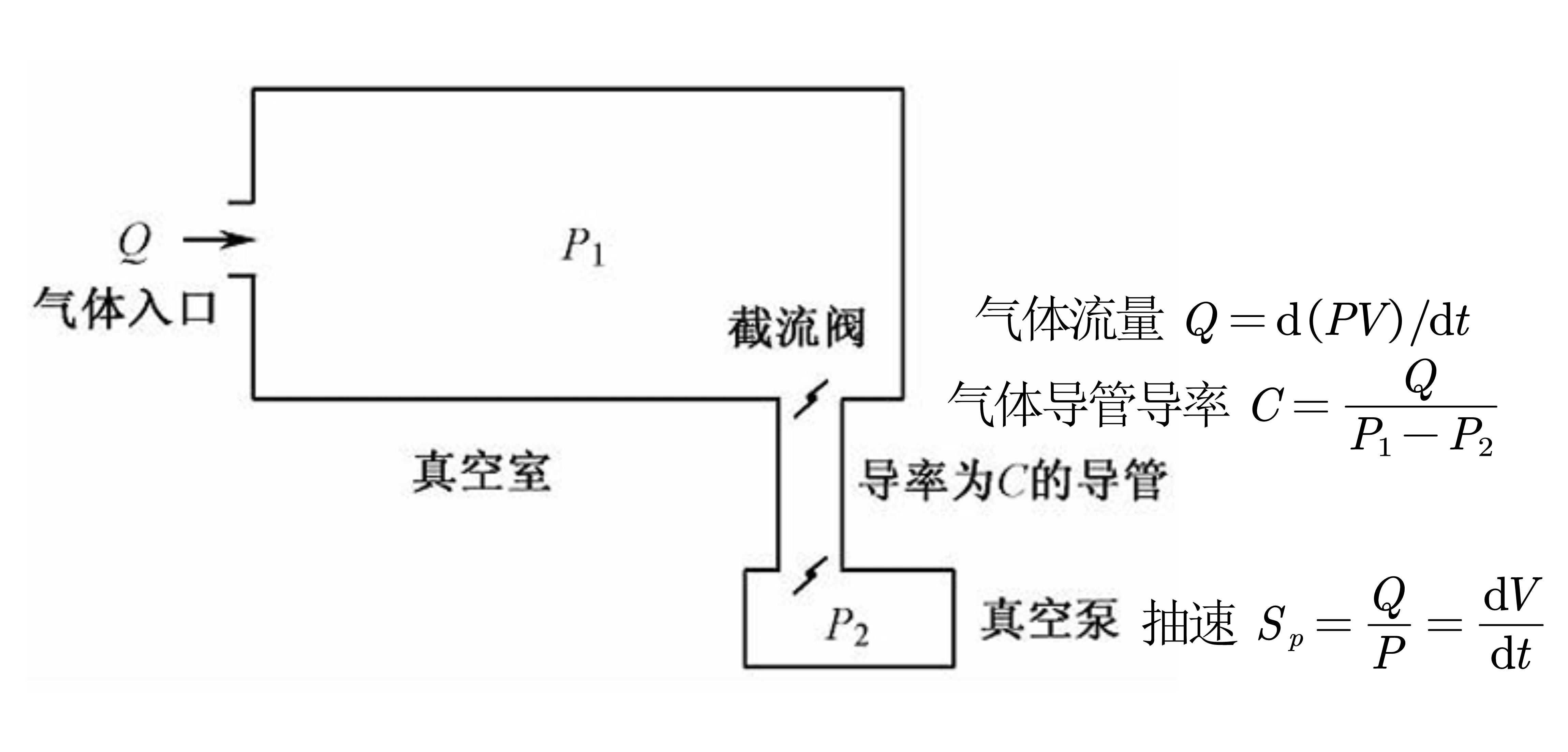
- 真空泵类型: 中低真空度用机械泵; 高真空者, 大流量用分子泵和扩散泵, 小流量用低温泵、升华泵
- 真空度测量: 中低真空度用电容压力计, 热偶规, 电离规, 更高的用B-A规(热阴极电离规), 复合真空计
- PVD工艺类型
- 真空蒸镀(Vacuum Evaporation):适合低熔点金属。在高真空室内加热源材料使之气化,源气相转移到达衬底,在衬底表面凝结形成薄膜
- 原理:


- 分类: 电阻蒸镀, 电子束蒸镀, 激光蒸镀
- 工艺: 准备->抽真空->预蒸->蒸发->取片
- 蒸镀为什么要求高真空度? 蒸发分子(或原子)的质量输运应为直线,若真空度过低,输运过程被气体分子多次散射,方向改变,动量降低,淀积的薄膜疏松、致密度低; 真空度低,气体中的氧和水汽,使蒸发的金属原子在气相就被氧化,淀积的薄膜成为氧化物薄膜; 若真空室中有较多气体杂质分子,它被蒸发原子流裹挟也淀积在衬底上,影响淀积薄膜纯度和质量。
- 如何改善step coverage? 衬底加热, 衬底旋转, 衬底支架设计为半球形
- 真空室基压、加热方式影响纯度, 衬底温度和蒸发速率影响粘附性; 蒸发快,薄膜纯度高且致密, 衬底粘附性好, 但薄膜表面不平
- 原理:
- 溅射(Sputtering):适合高熔点金属和合金。在一定真空度下,使气体等离子化,其中的离子轰击靶阴极,逸出靶原子等粒子气相转移到达衬底,在衬底表面淀积成膜
- 原理: 工作气体的等离子化->离子对靶的轰击->靶原子气相质量输运->淀积成膜
- 分类: 直流溅射 (只能制备导电的金属, 慢), 射频溅射 (支持电介质, 也慢), 磁控溅射 (只能制备导电的, 纯度提升损伤少), 反应溅射 (气体与靶材化学反应, 制备化合物), 偏压溅射 (更纯更密更结实, 有缺陷), 离子束溅射 (高质量)
- 溅射与蒸镀薄膜质量的比较: 溅射 保形覆盖+附着性+致密性好, 膜厚可控性和重复性好; 纯度较高,不存在蒸镀时无法避免的坩埚污染现象; 慢, 在制备特殊材质薄膜上不如电子束蒸镀, 但衬底辐射造成的缺陷少
- 后面乱七八糟举了点例子不想看了
- 真空蒸镀(Vacuum Evaporation):适合低熔点金属。在高真空室内加热源材料使之气化,源气相转移到达衬底,在衬底表面凝结形成薄膜
Lecture 8: CMOS-MEMS集成技术
- CMOS-MEMS集成
- 将MEMS结构与CMOS电路集成在同一芯片上, 高集成度、低成本、高性能
- Post CMOS-MEMS, Pre CMOS-MEMS, Inter CMOS-MEMS (MEMS出现在前道工艺, 后道工艺还是中间)
- MEMS制造工艺
bulk micromachining (深厚) 与 surface micromachining (浅薄)- 薄膜沉积(Thin-film Deposition):CVD、PVD等。
- 光刻与刻蚀(Lithography and Etching):定义MEMS结构。
- 释放工艺(Release Process):去除牺牲层,释放可动结构。